THELYOS
A New Generation of Thermal Analysis for Microelectronics

Benefits
- Higher spatial resolution
- Higher temperature resolution
Key words
- Hot spot detection
- Scanning thermal microscopy
- Temperature mapping
Laboratory
- NEEL
Institutions
- CNRS
- GRENOBLE INP-UGA
- UGA
Linksium Continuum
- Maturation
- Incubation
Results
- Incorporated startups
Context
Modern microelectronics faces a major challenge: identifying and understanding electrical or physical failures that lead to hot spots within circuits. These localized areas of high current density degrade both the performance and the reliability of devices.
Detecting such phenomena at the nanoscale requires local, precise, and highly sensitive measurement tools capable of tracking heat dissipation at the heart of active structures.
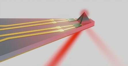
Thélyos introduces a new scanning thermal microscopy (SThM) instrument with unprecedented spatial and thermal sensitivity, surpassing all existing industrial solutions. It addresses several key challenges in today’s microelectronics:
- Optimizing thermal dissipation in high-current-density regions to enhance device performance.
- Meeting the challenges of miniaturization and energy efficiency in micro- and nanoscale components.
- Accelerating the development of energy conversion and recovery technologies (photovoltaic, thermoelectric) through precise characterization of the thermal conductivity of innovative materials.
Technology
Thélyos is based on a scanning thermal microscopy (SThM) platform that incorporates an ultra-sensitive resistive thermometer made of niobium nitride (NbN).
Resistive thermometry exploits the dependence of electrical resistance on temperature, characterized by the Temperature Coefficient of Resistance (TCR). The NbN sensor developed for Thélyos exhibits a TCR 5 to 10 times higher than that of existing technologies, providing exceptional thermal sensitivity.
The core innovation lies in the integration of the NbN thermometer directly onto three-dimensional AFM probes using electron-beam lithography — a complex process mastered exclusively by Institut Néel (CNRS).
Advantages
- Ultra-sensitive NbN thermometer with an excellent signal-to-noise ratio.
- Unmatched spatial and thermal resolution, ideally suited for nanoscale structures.
- Detection of extremely weak thermal fluxes, enabling detailed analysis of local heat transport phenomena.
- Enhanced measurement accuracy of thermal properties in nanoscale materials, structures, and devices.
State of progress
Fabrication process to integrate the NbN thermometer at the apex of the AFM tip has been optimized. We have calibrated NbN based thermal probes and demonstrated the sensitivity 5 times higher than the existing probes. Thermal measurements have been carried out on bulk and thin films. Next step, to adapt the process for batch fabrication of thermal probes.
Applications
Thélyos provides powerful capabilities for advanced characterization of nanoelectronic and optoelectronic devices, including:
- Detection and analysis of hot spots and failure mechanisms.
- In-plane thermal mapping of 3D chips and complex architectures.
- Measurement of thermal conductivity in nanoscale structures and devices.
- Characterization of phase-change materials.
- Investigation of heat transport in heterostructured nanomaterials.
- Detection of interconnect line narrowing caused by fabrication defects or electromigration.
- Thermal diagnostics of on-chip resistive elements.
Featured articles
 SERIAL TECH TRANSFR
1, 2 and 3 startups for Nora Dempsey, National Medal of Innovation 2021
Nora Dempsey is one of the four winners of National Medal for Innovation 2021 awarded by CNRS. Nora Dempsey, born in Ireland, has gained an international recognition for her research in Grenoble on...
Read the article PORTRAIT
Amiral Technologies, la startup IA grenobloise spécialisée dans les solutions de maintenance prédictive, intègre Station F
An ambitious promise: to invent a zero-defect and zero-downtime future for industry. Amiral Technologies, a startup co-founded and boosted by Linksium, based on the technological prowess of the Gre...
Read the article